Field: Technology
A material just one atom thick reveals a strange quantum secret
Published | Technical Staff
Visualization
In a groundbreaking investigation into the peculiar behavior of electrons, researchers at the University of Osaka have unveiled a new quantum state at the interface between a one-atom-thick material and a metallic substrate. This discovery offers deep insights into the realm of heavy fermions, where electrons display attributes akin to an increased mass that leads to remarkable quantum phenomena such as unconventional superconductivity.
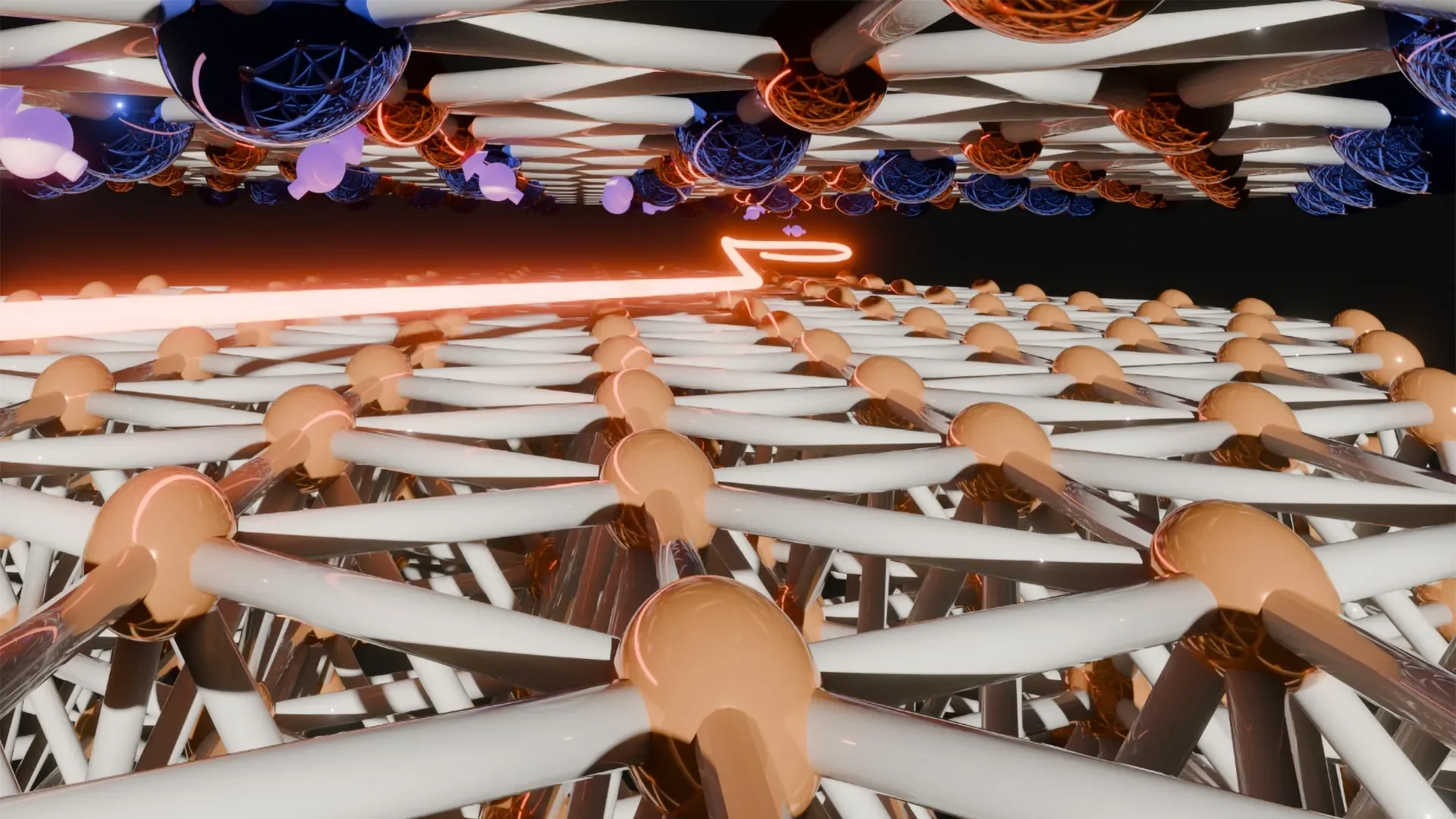
The experimental setup designed by the Osaka team involved creating a precisely engineered atomic layer of ytterbium copper, specifically YbCu₂, situated atop a crystalline copper surface. To probe this emergent heavy fermion behavior, the scientists employed advanced synchrotron radiation techniques, allowing them to scrutinize the intricate interactions of electrons at the boundary of these two materials. The resultant measurements revealed an interaction that diverged dramatically from classical expectations, with electrons in the thin Yb layer interacting selectively with the delocalized conduction electrons inhabiting the copper substrate underneath.
Notably, two distinct heavy fermion states were identified during this exploration. The first state was confined predominantly within the two-dimensional confines of the ytterbium layer, whereas the second extended into the threedimensional lattice of the copper crystal, marking a significant milestone whereby heavy fermion behavior was found at a material interface—a phenomenon that had not been observed thus far in this particular system.
The origins of this interaction can be traced back to the hybridization of 4f electrons from ytterbium, which are typically localized owing to their correlation effects, with the more mobile conduction electrons present in the copper lattice. This hybridization produces an enhancement in effective mass for the electrons, causing them to behave as "heavy" fermions. Such electron interactions are visualized mathematically via the Kondo model, where the coupling strength between localized spins and conduction electrons can be expressed in Hamiltonian framework as \( H = -J \vec{S} \cdot \vec{s} \), with \( J \) representing the interaction strength, \( \vec{S} \) the localized spin, and \( \vec{s} \) the conduction electron spin density.
The implications of these findings extend beyond elucidating fundamental quantum mechanisms. Senior author Professor Shin-ichi Kimura emphasizes the potential of these interfacial regions to serve as engineering platforms for novel quantum states. By methodically manipulating the architecture of such interfaces—including careful selection of constituent materials and control over the electronic orbital arrangements—scientists can unlock new regimes of quantum behavior. This could herald a new epoch in the design of materials exhibiting unprecedented electronic properties and functionalities.
Future lines of inquiry will likely delve into the enhancement of interfacial interactions through strain engineering or the exploration of moiré patterns that emerge from overlapping atomic arrangements. These efforts could lead to a deeper understanding of quantum materials physics and may lay the groundwork for applications involving quantum computation and the realization of room-temperature superconducting materials.
As the researchers continue to refine their methods and probe the boundaries of material science, it is evident that the intricate dance of electrons at the atomic scale harbors secrets yet untold—waiting just beyond the reach of our conventional understanding, poised to revolutionize technology for years to come.
The experimental setup designed by the Osaka team involved creating a precisely engineered atomic layer of ytterbium copper, specifically YbCu₂, situated atop a crystalline copper surface. To probe this emergent heavy fermion behavior, the scientists employed advanced synchrotron radiation techniques, allowing them to scrutinize the intricate interactions of electrons at the boundary of these two materials. The resultant measurements revealed an interaction that diverged dramatically from classical expectations, with electrons in the thin Yb layer interacting selectively with the delocalized conduction electrons inhabiting the copper substrate underneath.
Notably, two distinct heavy fermion states were identified during this exploration. The first state was confined predominantly within the two-dimensional confines of the ytterbium layer, whereas the second extended into the threedimensional lattice of the copper crystal, marking a significant milestone whereby heavy fermion behavior was found at a material interface—a phenomenon that had not been observed thus far in this particular system.
The origins of this interaction can be traced back to the hybridization of 4f electrons from ytterbium, which are typically localized owing to their correlation effects, with the more mobile conduction electrons present in the copper lattice. This hybridization produces an enhancement in effective mass for the electrons, causing them to behave as "heavy" fermions. Such electron interactions are visualized mathematically via the Kondo model, where the coupling strength between localized spins and conduction electrons can be expressed in Hamiltonian framework as \( H = -J \vec{S} \cdot \vec{s} \), with \( J \) representing the interaction strength, \( \vec{S} \) the localized spin, and \( \vec{s} \) the conduction electron spin density.
The implications of these findings extend beyond elucidating fundamental quantum mechanisms. Senior author Professor Shin-ichi Kimura emphasizes the potential of these interfacial regions to serve as engineering platforms for novel quantum states. By methodically manipulating the architecture of such interfaces—including careful selection of constituent materials and control over the electronic orbital arrangements—scientists can unlock new regimes of quantum behavior. This could herald a new epoch in the design of materials exhibiting unprecedented electronic properties and functionalities.
Future lines of inquiry will likely delve into the enhancement of interfacial interactions through strain engineering or the exploration of moiré patterns that emerge from overlapping atomic arrangements. These efforts could lead to a deeper understanding of quantum materials physics and may lay the groundwork for applications involving quantum computation and the realization of room-temperature superconducting materials.
As the researchers continue to refine their methods and probe the boundaries of material science, it is evident that the intricate dance of electrons at the atomic scale harbors secrets yet untold—waiting just beyond the reach of our conventional understanding, poised to revolutionize technology for years to come.